


Video
Step-by-Step PCB design Guide
From the initial drawings to the final files, here are the 9 steps toward designing a Printed Circuit Board:
1. Understand the electrical parameters.
Before starting a PCB design, you should know and understand the electrical parameters of the system, including:
Current maximums
Voltages
Signal types
Capacitance limitations
Impedance characteristics
Shielding considerations
Type and location of circuit components and connectors
Detailed net wire listing and schematic
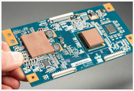
2. Creating the schematic.
One of the first steps is always creating a schematic, which refers to the design at the electrical level of the board’s purpose and function. At this point, it’s not yet a mechanical representation.
3. Use a schematic capture tool to create your PCB layout.
The right PCB provider will work with principal engineers to develop a schematic with a software platform such as Mentor PADS®, Allegro, or Altium, which shows you exactly how your board will operate and where the components will be placed. After you create your schematic, the mechanical engineer will load the design and determine how it will fit in the intended device.
4. Design your PCB stackup.
This is important to consider early on in the PCB design stage due to impedance, which refers to how much and how quickly electricity can travel down a trace. The stackup plays a role in how the mechanical engineer can design and fit the PCB into the device.
5. Define design rules and requirements.
This step is largely dictated by standards and acceptability criteria from the IPC, which is the industry association for PCB and electronics manufacturing. These standards tell you everything you need to know regarding PCB Manufacturing. An important tip: Find a PCB layout provider who is extremely familiar with IPC standards; this can help you avoid major revisions and project delays.
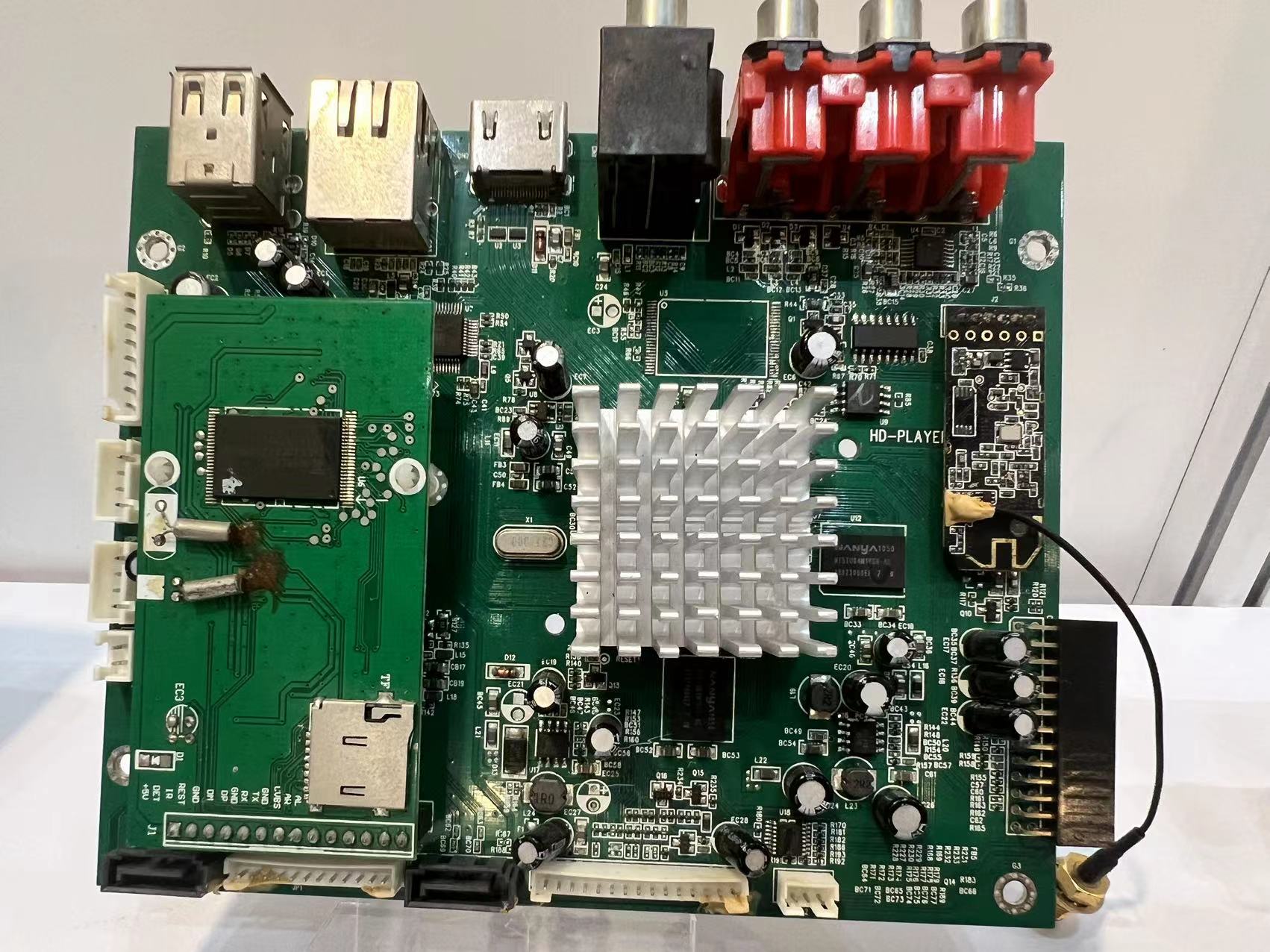
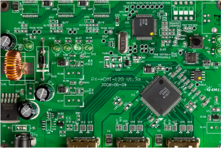
6. Place your components.
In many cases, the customer and PCB provider will discuss design and layout guidelines when it comes to the placement of components. For example, there may be standards indicating that certain components cannot be placed near others because they create electrical noise in the circuit. The PCB provider will have data sheets on every component (in most cases these are connectors), which will then be placed in the mechanical layout and sent to the customer for approval.
7. Insert drill holes.
This step is driven by the components and a connection. About half of the flex circuits on the market are double-sided, which means they have connection to the drill hole on the bottom layer.
8. Route the traces.
After you’ve placed the components and drill holes, you’re ready to route the traces, which means connecting segments of the path.
9. Add labels and identifiers.
Now is the time to add any labels, identifiers, markings, or reference designators to the layout. Reference designators are helpful in showing where specific components will go on the board.
10. Generate design/layout files.
This is the final step in the layout process. These files contain all the information pertaining to your printed circuit board, and once they have been generated, your PCB is now ready for fabrication and manufacturing and assembly.
Related articles
What are single sided PCBs?
What are single sided PCBs? Single sided printed circuit boards are circuit boards with one layer of conducting material on one side of the board, while the other side is used for incorporating d...
![[video]What is a printed circuit board?](https://xzhems.com/zb_users/upload/2023/03/202303071678178509507120.png)
[video]What is a printed circuit board?
What is a Printed Circuit Board?A printed circuit board, or PC board, or PCB, is a non-conductive material with conductive lines printed or etched. Electronic components are mounted on the board and t...
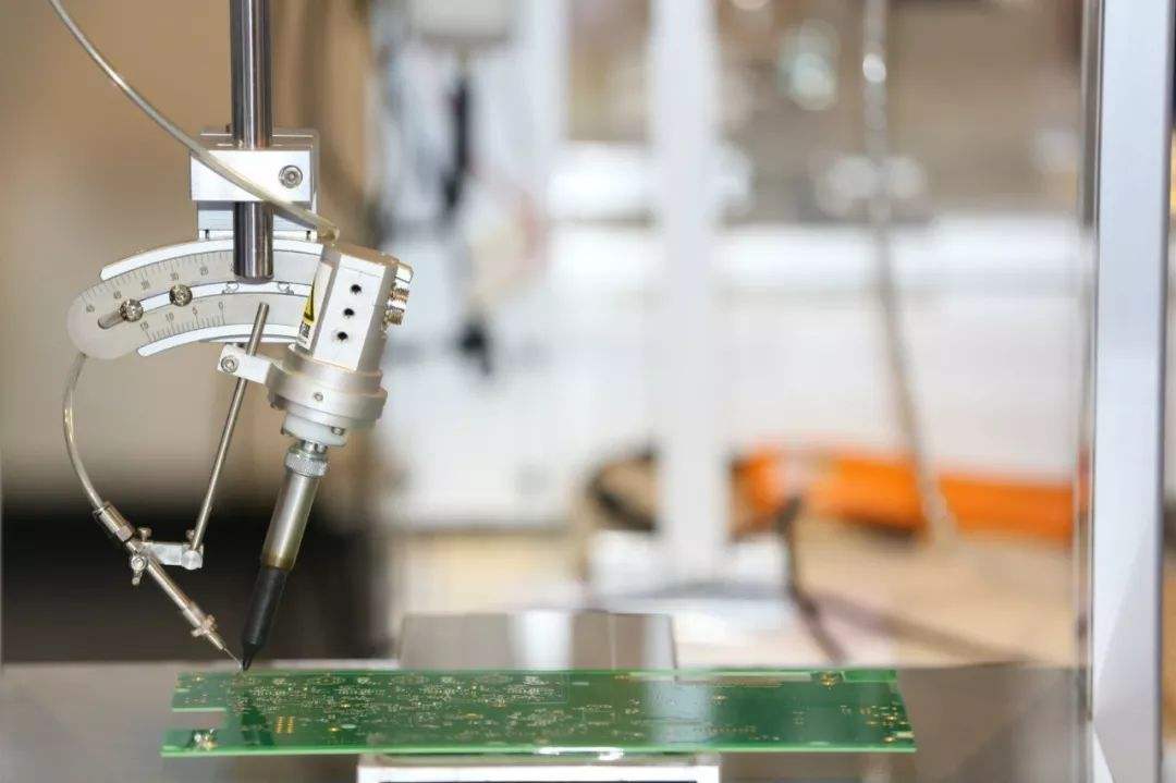
Video:How To Test a PCBA (Printed Circuit Board Assembly)
Video:How To Test a PCBA (Printed Circuit Board Assembly)In this Video , mainly talks about cracks in the PCBs and shows how Micro-Measurements strain gage sensors are used when testing components, su...
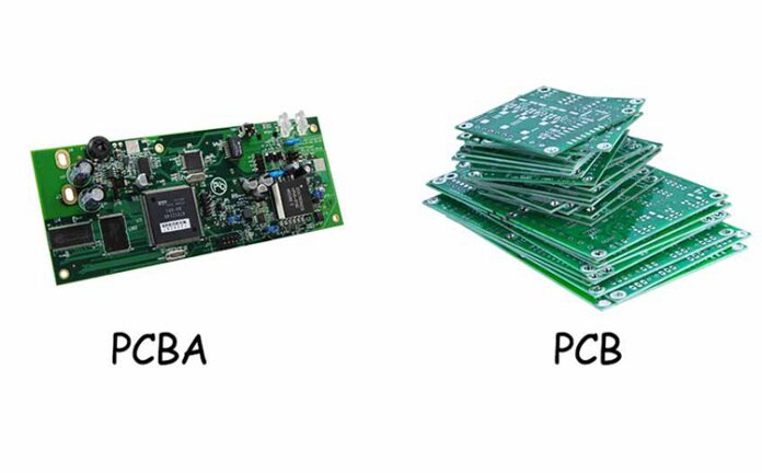
what is pcba meaning?
what is pcba meaning?PCBA is printed circuit board assembly.A printed circuit board assembly (PCBA) describes the finished board after all the components have been soldered and installed on a pri...
Video:Difference Between PCB and Printed Circuit Board Assembly
Use a video to explain the difference between PCB and PCBA.Reference description of videoThe Youtube author of the video titled "PCB Vs PCBA | Difference Between PCB and Printed Circuit Board Ass...
![[video]A leading PCB manufacturer of PCB Manufacturing](https://xzhems.com/zb_users/upload/2023/03/202303071678183115458149.png)
[video]A leading PCB manufacturer of PCB Manufacturing
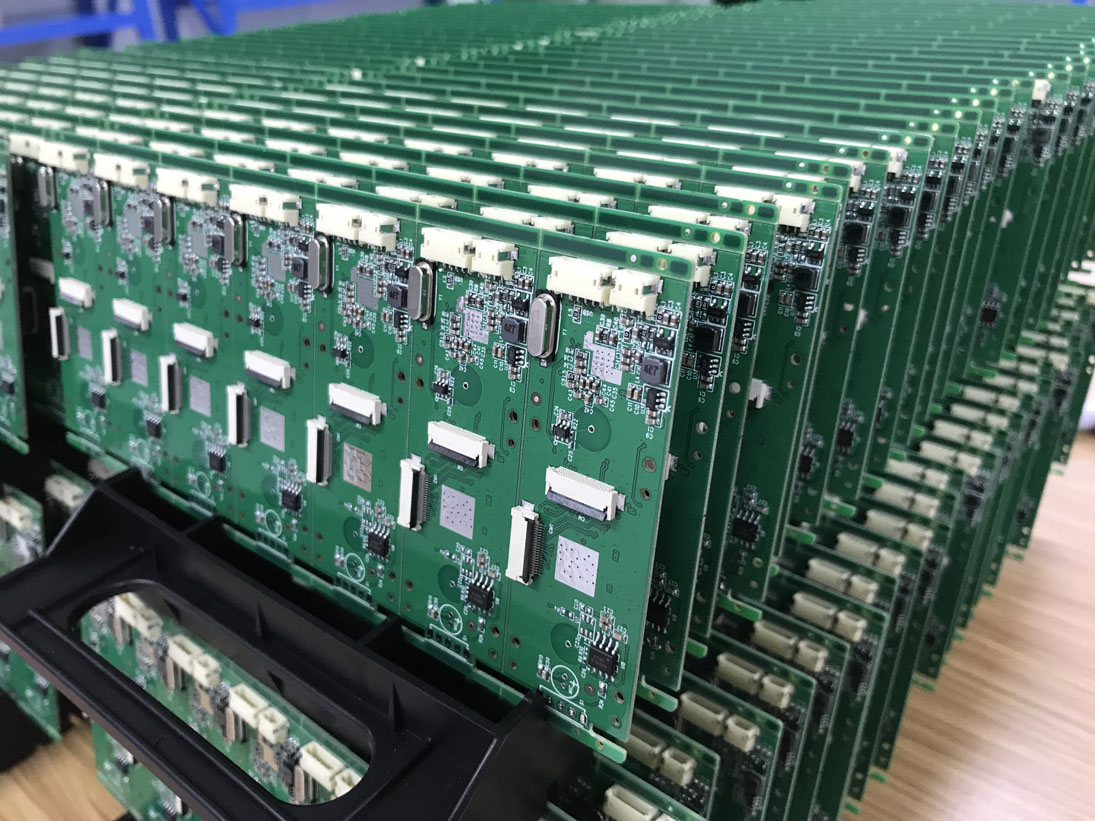
Xinzhanhong is a professional Printed Circuit Board Manufacturing and assembly factory, providing one-stop PCBA customization service for customers....
Leave a comment
